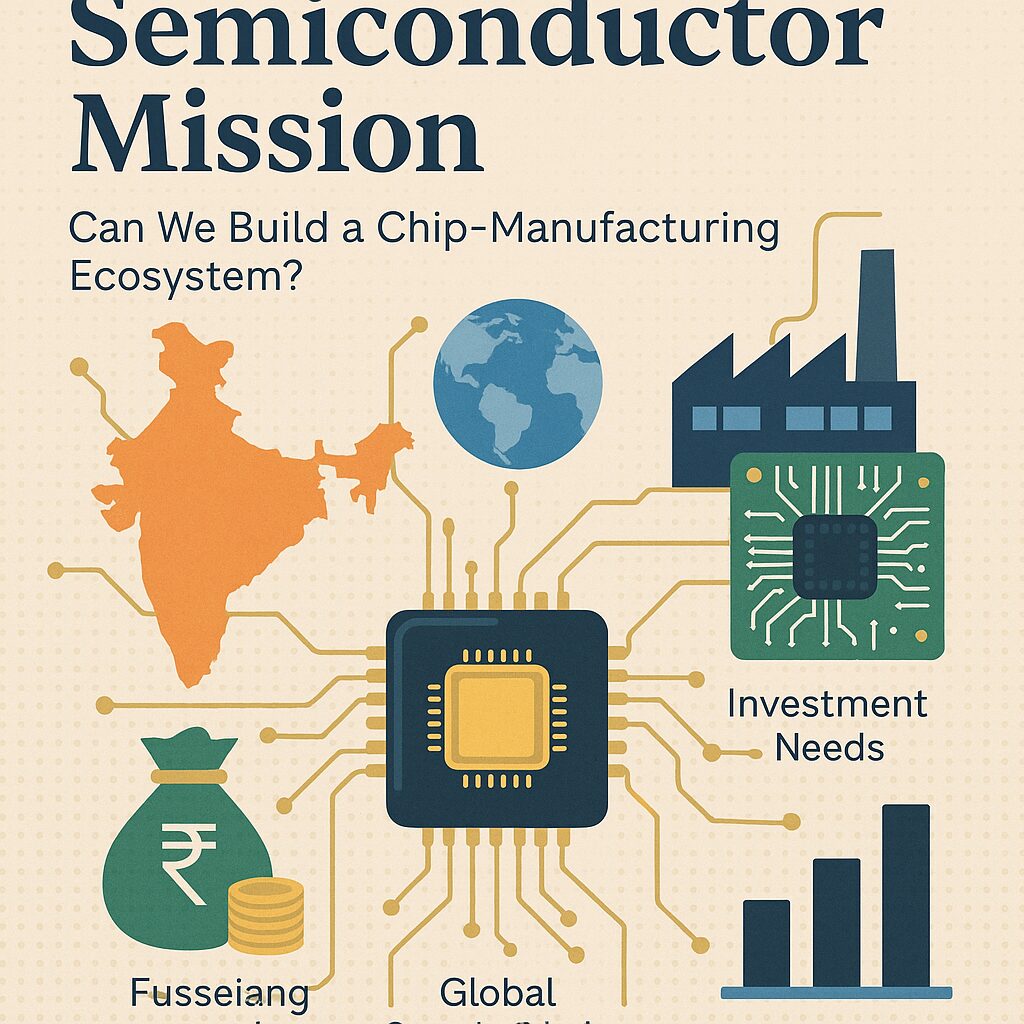
India’s Semiconductor Mission: Can We Build a Chip-Manufacturing Ecosystem?
Assessing India’s ambition to become self-reliant in semiconductors, the global supply-chain shifts, and investment needs.
Executive summary
India has moved from aspiration to execution on chips. Since mid-2023, New Delhi has put in place a 50% capital subsidy for fabs and advanced packaging, fast-tracked approvals, and green-lit a first logic 28-nm foundry by Tata Electronics with Powerchip (PSMC) in Dholera, Gujarat, plus two OSAT/ATMP plants (Tata TSAT in Assam and CG Power with Renesas & Stars Micro in Sanand) and Micron’s DRAM/NAND assembly-test complex in Sanand. Together these signal a credible first wave concentrated in the Sanand–Dholera–Assam corridor, with timelines that—if met—would see India ship its first home-fabricated wafers in the second half of 2026 and reach meaningful packaging output earlier. Press Information Bureau+1
Global dynamics are unusually favorable. The U.S. CHIPS and Science Act (2022) mobilizes $52.7 billion in direct funding and incentives; the EU and Japan have responded with their own packages; and TSMC, Intel, Samsung, Micron, GlobalFoundries, Amkor and others are regionalizing capacity, often at mature and mid-nodes relevant to India’s auto, industrial and power-electronics base. Reuters+3Wikipedia+3manufacturingdive.com+3
India’s challenge isn’t whether to invest, but how to sequence: start where the country can win quickly (OSAT/ATMP, power management ICs, MCU/analog, specialty and 28 nm logic), build tight supplier clusters around Gujarat and a second hub in the east/northeast, scale talent (design + manufacturing), guarantee utilities (power, ultrapure water, gas) on world-class SLAs, and de-risk with long-term anchor demand (automotive, railways, power, telecom, defence). The fiscal math is significant: a single 50k-WSPM 28-nm fab costs on the order of ₹91,000 crore (~$11 billion); a mid-to-large OSAT is ₹7,600–27,000 crore ($0.9–3.2 billion)—hence the need for central + state co-financing, anchor offtake, and export-linked performance metrics. Press Information Bureau
The payoff is also significant. India already holds ~20% of the world’s semiconductor design engineers, a rare strength most new entrants lack. Converting design depth into manufacturing presence—starting with packaging and mature-node logic/analogue—can anchor supply security for India’s $100-billion-by-2030 semiconductor consumption and catalyze electronic manufacturing scale. ITIF
1) The global context: why the window is open now
Policy tailwinds.
- United States: The CHIPS and Science Act appropriates $52.7 billion (grants, loans, R&D) and a 25% investment tax credit. Awards across 2024–2025 span Intel, TSMC (Arizona), Samsung (Texas), GlobalWafers (wafers), Amkor (advanced packaging), etc.—all evidence of a structural push to re-shore or friend-shore capacity. Reuters+3Wikipedia+3The Verge+3
- European Union/Germany: The EU Chips Act mobilizes €43 billion (public + private). Germany has backed Intel’s Magdeburg fab and TSMC’s Dresden consortium with multibillion-euro packages, despite delays—again showing Europe’s determination to own critical capacity. Embedded+2Bloomberg+2
- Japan: The government has funded TSMC’s Kumamoto fabs and Rapidus (2 nm) with multibillion-dollar support, coupling advanced packaging R&D with production subsidies—an explicit template for late-mover catch-up. pr.tsmc.com+2Reuters+2
Industrial shift: mature nodes matter.
While media attention fixates on 3 nm or 2 nm, supply risk is acute at mature nodes (40–90 nm, 28 nm) used in autos, industrial controls, power and connectivity. TSMC’s 4-nm ramp in Arizona and Japan’s 12/16–40 nm in Kumamoto prove that regionalization is landing exactly where India wants to play first. Reuters+1
Packaging resurges.
Advanced packaging (flip-chip, fan-out, heterogeneous integration) is now strategic. The U.S. has funded Amkor Arizona; Japan and the EU have similar efforts; and India is rightly seeding OSATs alongside the fab. Reuters
2) India’s policy architecture: from vision to projects
Semicon India Programme (Dec 2021; outlay ₹76,000 crore) and the Modified Schemes provide 50% fiscal supportfor CMOS fabs, display fabs, compound/sephotonics/sensors/discretes, and ATMP/OSAT—a generous, pari-passustructure aligned with global peers. Press Information Bureau+1
Approvals & first wave (as of Feb 29, 2024; updated through 2025 developments):
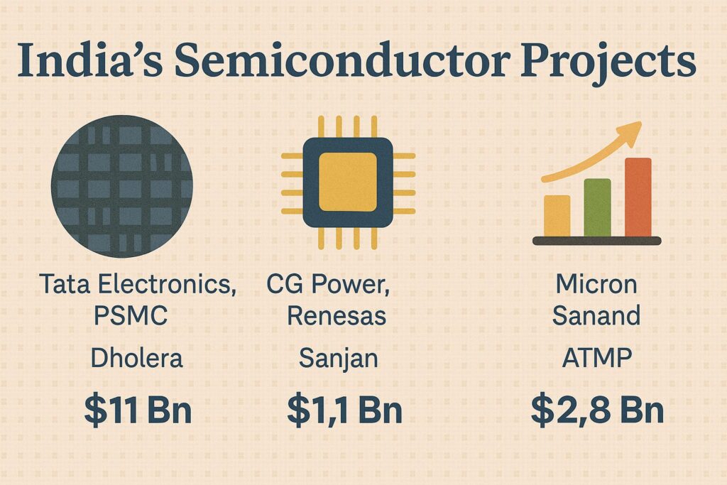
- Tata Electronics + PSMC 28-nm fab, Dholera (Gujarat): Capacity 50k WSPM; capex ₹91,000 crore; segments: 28-nm logic/HPC and power-management ICs; construction launched with an aggressive schedule targeting first chips by late-2026 per public statements. Press Information Bureau+1
- Tata TSAT OSAT, Morigaon (Assam): Capex ₹27,000 crore; advanced packaging (flip-chip, integrated system-in-package). Press Information Bureau
- CG Power–Renesas–Stars Micro OSAT, Sanand (Gujarat): Capex ₹7,600 crore; focus on consumer/industrial/automotive/power chips. Commissioning milestones reported across 2025, including pilot-line inauguration. Press Information Bureau+1
- Micron ATMP, Sanand (Gujarat): Total project up to $2.75 billion (with central 50% + state support; Micron equity up to $825 million). Phase-1 cleanroom ~500,000 sq ft; staged operations from late-2024 into 2025 per company. Micron Technology
Together, these create a practical ladder: start with assembly/test and mature-node logic/analog, build supplier density, and progress to specialty and more advanced nodes when yields, skills and demand justify.
3) India’s starting advantages—and gaps to close
Design talent & GCC depth.
Multiple credible sources (policy, think-tank, and industry trackers) place ~20% of global chip design engineers in India—125,000+ professionals—distributed across GCCs of Intel, Qualcomm, Nvidia, Broadcom, MediaTek, NXP, TI, AMD, and fabless startups. This is rare leverage: most late entrants lack design-to-manufacturing feedback loops. ITIF
Demand gravity.
India’s chip consumption is projected to exceed $100 billion by ~2030, powered by smartphones, automotive electronics (EVs/ADAS), power/industrial, telecom, defence and consumer IoT. Locking in even a 15–25% local value-add materially impacts the current account and supply security. Zetamicron
Gaps:
- Manufacturing yield know-how, defect-density control, and automotive-grade qualifications (AEC-Q100, IATF 16949) across foundry and OSAT.
- Supplier stack (CMP slurries, photoresists, high-purity gases/chemicals, silicon wafers) and critical sparesavailability.
- Utilities at fab-grade SLAs: power quality/backup, UPW (ultra-pure water), waste treatment and zero-liquid discharge; fast customs for tools/spares.
- Workforce breadth beyond design: process, equipment, yield, facilities, EHS, and high-volume operations culture.
4) What the first Indian fabs/OSATs will actually make (and why that’s smart)
28-nm logic + power-management ICs (PMICs) can serve:
- Automotive (body, chassis, infotainment, powertrain domain controllers at mature nodes)
- Industrial & Power (motor drives, PLCs, solar/wind inverters, grid-edge power electronics)
- Telecom & Consumer (RF front-ends, PMICs, connectivity)
The Tata-PSMC fab’s stated 28-nm + power portfolio aligns with India’s fastest-growing electronics verticals, while being realistic about tooling, process IP and yield learning curves. On packaging, flip-chip and SiP are high-value and sticky, enabling India-made modules for automotive/industrial where reliability and traceability matter as much as node size. Press Information Bureau
5) Investment needs: realistic numbers & phasing
Capital envelopes (approved projects)
- Logic fab (Dholera, 50k WSPM, 28 nm): ₹91,000 crore (~$11 billion).
- OSAT (Assam, Tata TSAT): ₹27,000 crore (~$3.2 billion).
- OSAT (Sanand, CG Power JV): ₹7,600 crore (~$0.9 billion).
- Memory ATMP (Micron, Sanand): Up to $2.75 billion two-phase program. Press Information Bureau+1
How the subsidy works
India’s scheme provides 50% of project cost pari-passu from the Centre, with additional state incentives (land, stamp duty, power/water subsidies, capex top-ups). This mirrors CHIPS-style blended finance globally and is table stakes for first-of-kind entrants. Press Information Bureau
Opex expectations
Fabs are energy-, water- and consumables-intensive. Even at mature nodes, chemicals/gases, targets, resists, spares and scrubber media are recurring high-ticket items. Packaging lines require epoxies, underfills, substrates, leadframes, with costs sensitive to substrate cycles. Early-years opex will be above steady-state until yields stabilize (typically 18–30 months).
Financing structure
- Equity (sponsor + strategic tech partner)
- Subsidy tranches against capex milestones
- Long-tenor debt (multilateral, export-credit where tools are imported)
- Anchor offtake (auto/industrial OEMs, PSU demand aggregation for power/rail/defence) to derisk utilization
6) Timelines, milestones, and credible targets (2024–2030)
- 2024–2025: Build-out of Micron ATMP (cleanroom validated 2025), CG-Renesas OSAT pilot line inaugurated (Aug 2025); Tata Assam OSAT phases staggered; Dholera fab construction in full swing. The Economic Times+1
- Mid-2025 to 2026: Initial OSAT high-mix output ramps; automotive-grade certification flows begin.
- Late-2026: First 28-nm wafer output from Dholera targeted per ministerial statements. The Economic Times
- 2027–2030: Second-wave expansions (specialty nodes, compound semiconductors, advanced packaging lines) contingent on yields, supplier localization and export wins.
These are ambitious but plausible if (i) cluster utilities are flawless, (ii) tech-transfer staff rotations with PSMC/partners scale up, and (iii) customs/spares logistics are expedited.
7) Talent: the decisive variable
Design base is a strength (~20% global share), but manufacturing talent (process/equipment/yield/facilities/EHS/QA) needs scaling. Government programs (Chips-to-Startup, AICTE’s VLSI curriculum, SMART/NIELIT) target 85,000 design-side trainees over a decade and broader upskilling; companies are seconding hundreds of engineers to Taiwan and Japan for on-the-job training. Press Information Bureau+1
What to add quickly
- Dual-track academies inside Sanand–Dholera (8–12 week bootcamps + 12-month apprenticeships).
- Academic pilot lines for unit processes (deposition, litho, etch, metrology) to produce hands-on operators.
- Scholarships with return-service clauses; targeted women-in-semiconductor programs to lift participation beyond current baselines. India Briefing
8) Supply-chain localization: what must cluster inside India (and what can be imported first)
Must-have in India by 2027:
- Critical gases (N₂, O₂, Ar; specialty: NF₃, WF₆, SiH₄; abatement)
- Wet chemicals (H₂SO₄, H₂O₂, HCl, HF blends) at SEMI purity
- UPW systems, waste-treatment, slurry blending, CMP pads
- Advanced packaging substrates & leadframes (at scale)
- Cleanroom module fabrication & on-site maintenance (reduces MTTR)
Import-tolerant (short-term):
- Photoresists, EUV/ArF immersion materials (for when India moves below 28 nm)
- Front-end tools (duopolistic segments unlikely to localize soon)
Policy levers: green-channel customs for spares, bonded warehouses in-park, supplier tax credits and assured offtake; export-credit support for global vendors who co-locate.
9) Comparative lessons: U.S., EU, Japan—and what they imply for India
- Synchronize policy with project execution. The U.S. tied CHIPS awards to workforce plans, guardrails, and milestone-based disbursements; India’s 50% pari-passu support is comparable in generosity, but execution discipline (site readiness, SLAs, dispute-free land) will determine credibility. Wikipedia
- Start where industry demand is strongest. Japan backed Kumamoto at mature/mid nodes tied to auto/industrial customers; India’s 28 nm + PMIC strategy rhymes with this—stick to it before chasing <14 nm. pr.tsmc.com
- Packaging is strategic, not residual. The U.S. funded Amkor Arizona for advanced packaging; India’s dual-track OSAT push is right—scale it into a global service with reliability certifications and substrate capacity. Reuters
- Be realistic about breakthrough bets. Japan’s Rapidus shows the costs/risks of leaping to 2 nm from a standing start. India should partner for access to sub-14 nm via foundry alliances/overseas capacity while growing domestic nodes aligned to demand. Ministry of Economy, Trade and Industry+1
10) Risk map & mitigations
Yield and reliability risk.
- Mitigation: robust process-control & metrology investment; long-term on-site experts from PSMC/Renesas; supplier quality embedded in-park; automotive QA (PPAP, AEC-Q100) baked in from Day-1.
Utilities risk (power quality, UPW).
- Mitigation: dual power feeds with islandable backup; 24×7 on-site UPW technicians; ZLD with redundancy; service-level penalties for campus operators.
Talent churn.
- Mitigation: bonded training, competitive pay, rotation programs, and local universities inside the cluster.
Policy continuity & FX cycles.
- Mitigation: 8–10-year stability contracts; hedges; diversified customer mix with export orientation.
Global export controls/geopolitics.
- Mitigation: compliance-by-design; focus on mature nodes less exposed to controls; diversify tool suppliers.
11) Market linkage: who buys India-made chips first?
Prioritize domestic anchor demand that values reliability and proximity over nanometer prestige:
- Automotive & Mobility: 2-wheelers/3-wheelers, passenger cars (BS-VI/OBD-II), EV power & BMS, telematics.
- Energy & Power: inverters, smart meters, grid protection relays, charging infrastructure, rail traction.
- Industrial & Building: drives, HVAC controls, PLCs, access/security, elevators, robotics.
- Telecom & Defence: 4G/5G radios, satellite user terminals, radars, avionics LRU refresh.
Structure long-term supply agreements with Indian Tier-1s/PSUs and global OEMs manufacturing in India (auto, white goods, telecom) to underwrite utilization.
12) What success looks like by 2030 (a realistic scorecard)
- Two high-volume OSATs shipping at scale, with automotive certifications and export accounts.
- One mature-node logic fab (28 nm + power) at stabilized yields, ≥80% utilization, and roadmap to 40/65/90 nm analog/power variants.
- Supplier park in Sanand–Dholera with at least 50% of chemicals/gases by value made in India, plus substrateand leadframe lines.
- Manufacturing workforce of 25,000+ highly skilled fab/OSAT professionals; pipeline producing 10,000/year.
- Net import reduction measurable in auto/industrial/power electronics; export revenues from OSAT services and selected IC portfolios.
13) A sequenced roadmap (next 24–60 months)
Within 12 months
- Close supplier MoUs for UPW, gases, wet chemicals, substrates; set up in-park bonded warehouses.
- Launch cluster training center with PSMC/Renesas faculty; train first 1,000 technicians/operators.
- Sign anchor LTAs with top five Indian auto Tier-1s and two PSU clusters (power/rail).
12–24 months
- Complete tool install and facility qualification for OSAT-1/2; achieve >95% on-time delivery and <500 DPPMtargets in two product families.
- Dholera fab: ramp process modules (FEOL/BEOL), start engineering lots; stand up reliability labs (HTOL, temp cycle).
24–36 months
- Commercialize 28-nm & PMIC lines; start automotive PPAP flows; add SiC/GaN packaging pilot for power-electronics.
36–60 months
- Consider second fab module (or specialty analog/power line) once utilization >80% and two-year offtake secured; scale advanced SiP.
14) Frequently asked questions (with straight answers)
Q: Why not jump to 7 nm or below?
A: Cost and risk. Sub-10 nm requires EUV, massive supply-chain depth, and years of yield learning. 28 nm + analog/power serves India’s near-term demand and builds muscle without the EUV step; advanced packagingdelivers system-level performance now.
Q: Can India be globally competitive on cost?
A: Subsidies level the capex field. Operating cost competitiveness comes from cluster density (shorter supply lines), low downtime (fast spares), and high yields. With the right SLAs and supplier co-location, India can be cost-credible in OSAT and selected mature nodes.
Q: Is there enough talent?
A: On design, yes (~20% global). On manufacturing, not yet—but the combination of overseas rotations(Taiwan/Japan/US), cluster academies, and apprenticeships can bridge the gap in 2–3 years if executed at scale. ITIF+1
15) What India should not do
- Chase every node or every technology at once. Focus capital on mature logic/analogue/power and packaging, add SiC/GaN where India has power-electronics demand.
- Fragment into too many mini-parks. Double down on Sanand–Dholera (and one eastern hub) to get supplier density and talent flywheel.
- Under-invest in reliability & certification. Without automotive-grade credentials, domestic OEMs will hesitate to qualify parts.
- Neglect export orientation. Long-term competitiveness requires global customers and USD revenues.
16) Bottom line
The last two years changed the question from “Can India do chips?” to “Can India execute at scale?” The policy foundation (50% fiscal support), the first fab and three OSAT/ATMPs, and the design-talent base say yes—if we stay disciplined on nodes, build dense supplier parks, professionalize manufacturing talent, and lock anchor demand. Done right, by 2030 India is a credible packaging hub and mature-node logic/analogue maker—not a Taiwan or Korea, but a reliable third pillar in the global supply network for the electronics that power autos, energy, industry, and telecom.
17) Glossary of Terms
ATMP (Assembly, Testing, Marking & Packaging):
A stage in semiconductor manufacturing where chips fabricated on silicon wafers are cut, tested, and packaged for use in electronic devices.
OSAT (Outsourced Semiconductor Assembly and Test):
Third-party companies that provide assembly, packaging, and testing services for semiconductor firms. They play a crucial role in the global chip supply chain.
Fab (Fabrication Plant):
A manufacturing facility where semiconductor wafers are processed to create integrated circuits (ICs). Also referred to as a foundry.
Foundry:
A company or plant that manufactures chips designed by other companies (fabless firms). Example: TSMC, GlobalFoundries.
WSPM (Wafers per Month):
A metric to denote the capacity of a semiconductor fab, i.e., how many wafers it can process in a month.
Nanometer (nm) Node:
Refers to the technology generation of semiconductors, roughly indicating the size of transistors. Smaller nodes (e.g., 7 nm, 3 nm) allow more transistors per chip, improving performance and efficiency. Mature nodes like 28 nm are widely used in automotive and industrial applications.
28 nm Technology:
A widely used semiconductor manufacturing process node that balances performance, cost, and reliability. Essential for automotive, telecom, and industrial chips.
PMIC (Power Management Integrated Circuit):
A chip used to manage power requirements of the host system, ensuring efficiency, stability, and safety of electronic devices.
SiP (System-in-Package):
A type of packaging that integrates multiple ICs (logic, memory, sensors, RF) into a single package, offering performance and size benefits.
Flip-Chip Packaging:
An advanced packaging method where the semiconductor die is mounted upside down, directly connecting it to the substrate for better performance.
UPW (Ultra-Pure Water):
Specially treated water with extremely low contamination levels, critical for cleaning wafers in semiconductor fabs.
ZLD (Zero-Liquid Discharge):
A wastewater management process in fabs where no liquid waste is discharged, ensuring environmental compliance.
CMP (Chemical Mechanical Planarization):
A wafer-processing step that smooths and flattens surfaces using chemical and mechanical techniques.
EUV Lithography (Extreme Ultraviolet Lithography):
An advanced chipmaking process using very short wavelengths of light (13.5 nm) to etch smaller features on silicon wafers. Required for sub-7 nm nodes.
Analog Chips:
Semiconductors that process real-world signals like sound, light, and temperature, as opposed to purely digital data.
Compound Semiconductors (SiC, GaN):
Chips made from materials such as silicon carbide (SiC) or gallium nitride (GaN), offering high performance in power electronics and high-frequency devices.
PPAP (Production Part Approval Process):
A rigorous automotive industry standard to qualify suppliers and their components for use in vehicles.
AEC-Q100:
A reliability standard defined by the Automotive Electronics Council (AEC) for qualifying integrated circuits for automotive use.
IATF 16949:
An international quality management standard for automotive production and service parts organizations.
CHIPS and Science Act (USA):
A 2022 U.S. law providing $52.7 billion in subsidies and incentives to boost domestic semiconductor manufacturing and R&D.
EU Chips Act:
A European Union initiative mobilizing €43 billion in public and private funds to strengthen Europe’s semiconductor ecosystem.
Rapidus (Japan):
A Japanese consortium, heavily state-backed, tasked with developing advanced 2 nm semiconductor technology by the late 2020s.
PSMC (Powerchip Semiconductor Manufacturing Corporation):
A Taiwanese chipmaker partnering with Tata Electronics to build India’s first 28 nm fab.
Design-GCC (Global Capability Centers):
R&D and design offices set up in India by global semiconductor firms like Intel, Qualcomm, and Nvidia, employing thousands of engineers.
Pari-Passu Funding:
A financial structure where the government shares capital costs equally with industry partners (50:50), lowering private risk.
DPPM (Defective Parts Per Million):
A metric indicating the number of defective chips per million units shipped—a critical measure in automotive and high-reliability sectors.
18) References (selected)
- Government of India & ISM
- Cabinet approval (Feb 29, 2024): Tata-PSMC 28-nm fab (₹91,000 cr, 50k WSPM), Tata TSAT (₹27,000 cr, Assam), CG Power-Renesas-Stars OSAT (₹7,600 cr, Sanand). Press Information Bureau
- Semicon India (Modified Scheme): 50% fiscal support for CMOS fabs, display fabs, compound/sephotonics/discretes, and ATMP/OSAT. Press Information Bureau+1
- Project sponsors & status
- Micron India ATMP (Sanand): Up to $2.75 bn project; Micron equity up to $825 m; Phase-1 cleanroom 500k sq ft; staged ops 2024–25. Micron Technology
- CG Power OSAT—pilot line inauguration (Aug 2025) and market updates. Press Information Bureau+1
- Training & workforce initiatives (factsheet): targets for 85,000 design-side skilled manpower, AICTE curriculum changes. Press Information Bureau
- Global policy & market
- U.S. CHIPS & Science Act: $52.7 bn appropriations (grants, loans, R&D; 25% ITC). Wikipedia
- U.S. award tracker & company awards (TSMC, Samsung, TI, GlobalWafers, Amkor). Reuters+3manufacturingdive.com+3The Verge+3
- EU Chips Act (overview) & Germany subsidy cases (Intel Magdeburg, TSMC Dresden).Embedded+2Bloomberg+2
- Japan: TSMC Kumamoto & Rapidus 2 nm support. pr.tsmc.com+1
- India’s design-talent base
- ITIF (2024): India employs ~20% of the world’s chip design engineers. ITIF
19 ) A short, actionable checklist for policymakers & industry
- Lock utilities: legally binding power/water/gas SLAs; dual-feed, ZLD, on-site spares hubs.
- Stand-up supplier park: priority customs lane, bonded warehouses, and purchase-order visibility to co-located chemical/gas/substrate vendors.
- Talent at scale: 1,000+ apprentices per quarter per cluster; overseas rotations with return-service clauses; certification partnerships (IATF 16949, AEC-Q100).
- Anchor demand: long-term volume agreements with auto Tier-1s, energy PSUs, rail/metro, and telecom OEMs; “first-call” procurement for India-made packages/ICs that meet reliability specs.
- Export pipeline: dedicate business-development teams to qualify global mid-tier fabless firms and power-electronics leaders seeking redundant supply.
- Data discipline: publish quarterly cluster scorecards (yield, utilization, DPPM, cycle time) to sustain credibility with global customers and investors.
If India stays disciplined on these six levers, the first chips rolling out of Sanand–Dholera and Assam won’t be the end of a pilot—they’ll be the start of a durable manufacturing franchise that complements India’s world-class design engine and anchors a truly sovereign electronics future.
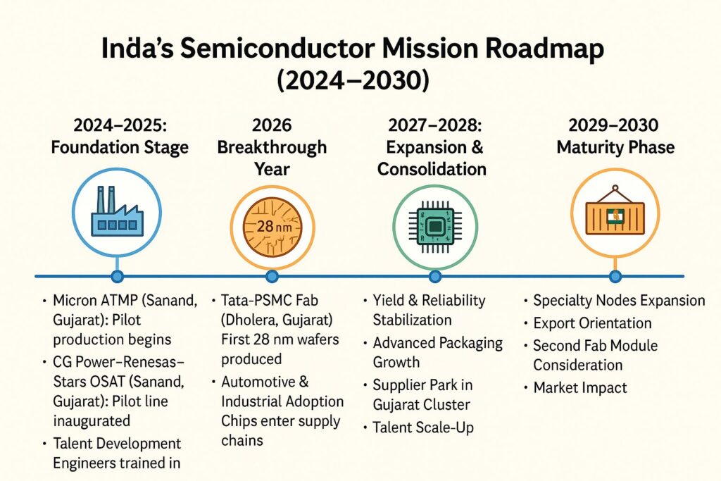
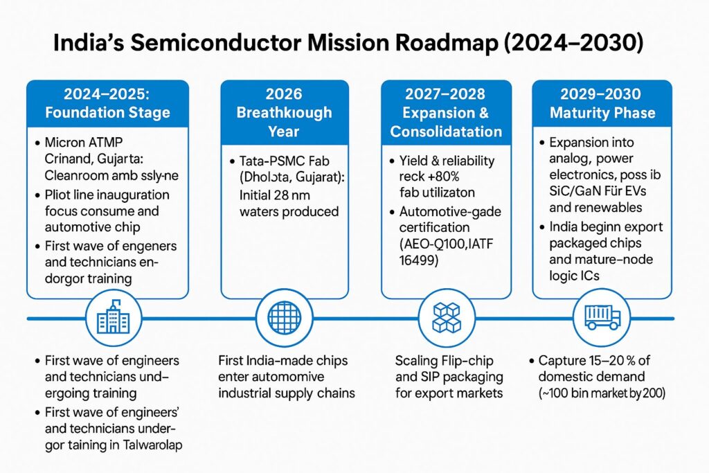
India’s Semiconductor Mission Roadmap (2024–2030)
2024 – 2025: Foundation Stage
- Micron ATMP (Sanand, Gujarat): Cleanroom and assembly-test lines commissioned, pilot production begins.
- CG Power–Renesas–Stars OSAT (Sanand, Gujarat): Pilot line inaugurated, focus on consumer and automotive chip packaging.
- Tata TSAT OSAT (Morigaon, Assam): Construction and phased rollout of advanced packaging facilities.
- Talent Development: First wave of engineers and technicians undergo training in Taiwan/Japan.
2026: Breakthrough Year
- Tata-PSMC Fab (Dholera, Gujarat):
- Initial 28 nm wafers produced.
- Ramp-up of power management ICs and mature-node logic chips.
- Automotive & Industrial Adoption: First India-made chips enter automotive and industrial supply chains.
2027 – 2028: Expansion & Consolidation
- Yield & Reliability Stabilization: Dholera fab reaches ~80% utilization with automotive-grade certification (AEC-Q100, IATF 16949).
- Advanced Packaging Growth: Flip-chip and SiP packaging scaled for export markets.
- Supplier Park: At least 50% of gases, chemicals, and substrates sourced locally in Gujarat cluster.
- Talent Scale-Up: Workforce exceeds 15,000 skilled fab/OSAT professionals.
2029 – 2030: Maturity Phase
- Specialty Nodes: Expansion into analog, power electronics, and possibly SiC/GaN for EVs and renewables.
- Export Orientation: India begins exporting packaged chips and mature-node logic ICs to global customers.
- Second Fab Module Consideration: Decision on new fab (40/65 nm analog/power or sub-28 nm node) based on demand and yields.
- Market Impact: India captures 15–20% of domestic demand (~$100 bn market by 2030), reduces import dependency, and becomes a global hub for packaging and mature-node logic.
Amulya Charan: It is a very comprehensively presented overview. I am just reminded of the Semi Conductor Complex (SCC) at Chandigarh that was built in the 1970s when we were just two generations behind the US in Chip technology. We never came to know who burnt it down to ashes so viciously that it could never be revived. Also the story of Texas Instruments trying to set up a semiconductor plant in India and their withdrawal following bureaucratic hassles indicates that we missed the Semiconductor boat deliberately. I am happy that pilot production in the facilities at Sanand have started. Work is progressing very rapidly at the Tata TSAT facility in Assam. I am not clear about the OSAT facility connected with the Tata venture in Assam where apparently third-party involvement is integrated into. Who these “third-parties” will be? These few months will be crucial to actually whether we are heading in the right direction in Semiconductors or not.
Thanks for going through my blog and giving detailed observations.